参考:
DDR3 控制器 MIG IP 详解完整版 (native&Vivado&Verilog)_mig ip核-CSDN博客
APP和AXI接口有许多相似的地方(握手部分),
但是由于和物理芯片直接相关,有更多不一样的地方。
addr的计算方式;
写命令和写数据到达时间可以各有前后等;
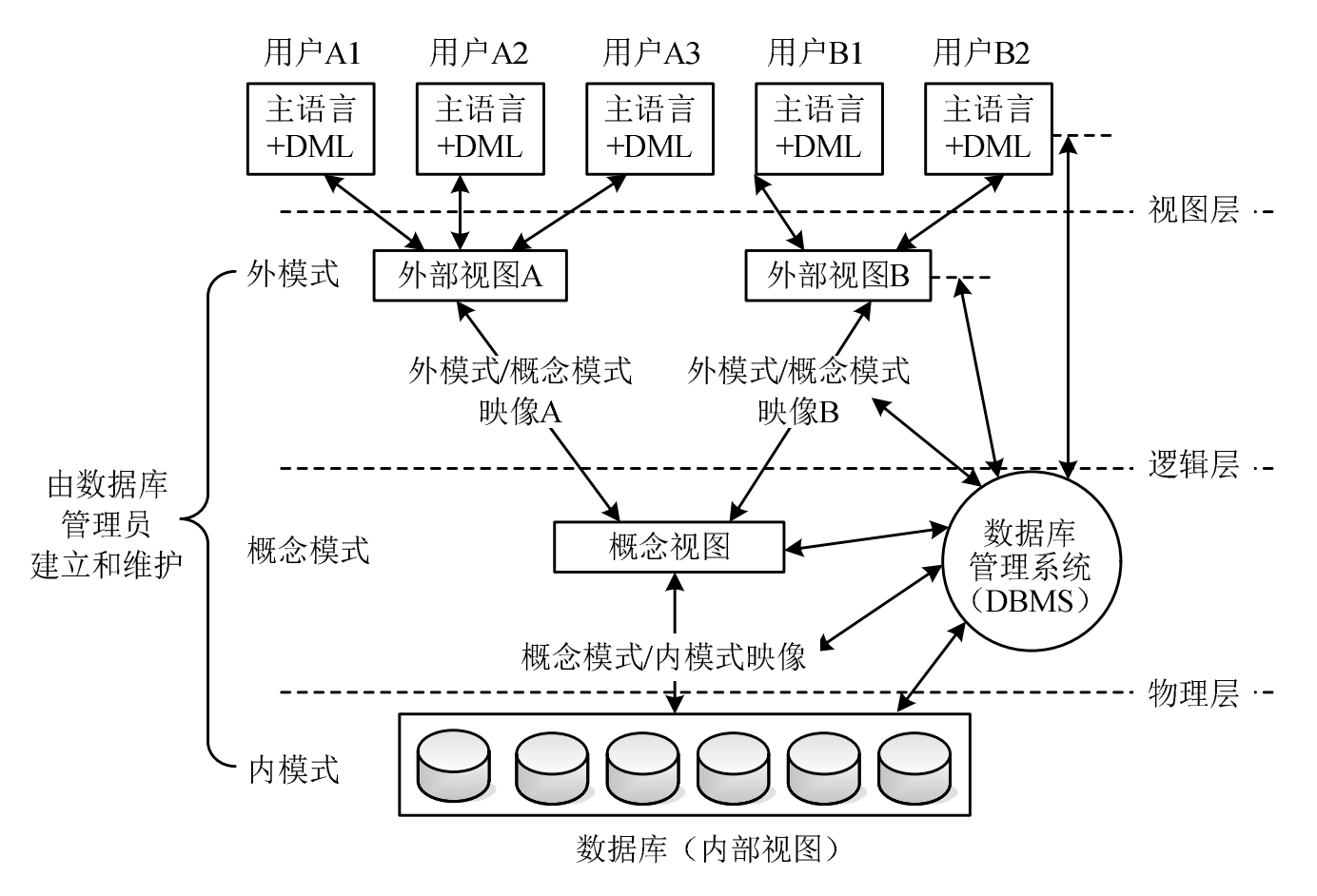
Memory Controller and Native Interface
The front end of the Memory Controller (MC) presents the native interface to the UI block. The native interface allows the user design to submit memory read and write requests and provides the mechanism to move data from the user design to the external memory device, and vice versa. The backend of the Memory Controller connects to the physical interface and handles all the interface requirements to that module. The Memory Controller also provides a reordering option that reorders received requests to optimize data throughput and latency.
内存控制器 (MC) 的前端向 UI 块提供本机接口。本机接口允许用户设计提交存储器读取和写入请求,并提供将数据从用户设计移动到外部存储器设备的机制,反之亦然。内存控制器的后端连接到物理接口并处理该模块的所有接口要求。内存控制器还提供重新排序选项,可以对收到的请求进行重新排序,以优化数据吞吐量和延迟。
IDELAYCTRL
An IDELAYCTRL is required in any bank that uses IDELAYs. IDELAYs are associated with the data group (DQ). Any bank/clock region that uses these signals require an IDELAYCTRL.
The MIG tool instantiates one IDELAYCTRL and then uses the IODELAY_GROUP attribute (see the iodelay_ctrl.v module). Based on this attribute, the Vivado Design Suite properly replicates IDELAYCTRLs as needed within the design.
The IDELAYCTRL reference frequency is set by the MIG tool to either 200 MHz, 300 MHz, or 400 MHz depending on memory interface frequency and speed grade of the FPGA. Based on the IODELAY_GROUP attribute that is set, the Vivado Design Suite replicates the IDELAYCTRLs for each region where the IDELAY blocks exist.
任何使用 IDELAY 的BANK都需要 IDELAYCTRL。 IDELAY 与数据组 (DQ) 关联。使用这些信号的任何存储体/时钟区域都需要 IDELAYCTRL。
MIG 工具实例化一个 IDELAYCTRL,然后使用 IODELAY_GROUP 属性(请参阅 iodelay_ctrl.v 模块)。基于此属性,Vivado Design Suite 根据设计中的需要正确复制 IDELAYCTRL。
MIG 工具将 IDELAYCTRL 参考频率设置为 200 MHz、300 MHz 或 400 MHz,具体取决于存储器接口频率和 FPGA 的速度等级。根据设置的 IODELAY_GROUP 属性,Vivado Design Suite 会为 IDELAY 块所在的每个区域复制 IDELAYCTRL。
基本接口信号:
  mig_7series_0 MIG_APP (
    // Memory interface ports
    .ddr3_addr                      ( ddr3_addr),            // output [13:0]	ddr3_addr
    .ddr3_ba                        ( ddr3_ba),              // output [2:0]		ddr3_ba
    .ddr3_cas_n                     ( ddr3_cas_n),           // output			ddr3_cas_n
    .ddr3_ck_n                      ( ddr3_ck_n),            // output [0:0]		ddr3_ck_n
    .ddr3_ck_p                      ( ddr3_ck_p),            // output [0:0]		ddr3_ck_p
    .ddr3_cke                       ( ddr3_cke),             // output [0:0]		ddr3_cke
    .ddr3_ras_n                     ( ddr3_ras_n),           // output			ddr3_ras_n
    .ddr3_reset_n                   ( ddr3_reset_n),         // output			ddr3_reset_n
    .ddr3_we_n                      ( ddr3_we_n),            // output			ddr3_we_n
    .ddr3_dq                        ( ddr3_dq),              // inout [31:0]		ddr3_dq
    .ddr3_dqs_n                     ( ddr3_dqs_n),           // inout [3:0]		ddr3_dqs_n
    .ddr3_dqs_p                     ( ddr3_dqs_p),           // inout [3:0]		ddr3_dqs_p
    .init_calib_complete            ( init_calib_complete),  // output			init_calib_complete
	.ddr3_cs_n                      ( ddr3_cs_n),            // output [0:0]		ddr3_cs_n
    .ddr3_dm                        ( ddr3_dm),              // output [3:0]		ddr3_dm
    .ddr3_odt                       ( ddr3_odt),             // output [0:0]		ddr3_odt
    // Application interface ports
    .app_addr                       ( app_addr           ),  // input [27:0]		app_addr
    .app_cmd                        ( app_cmd            ),  // input [2:0]		app_cmd
    .app_en                         ( app_en             ),  // input			app_en            MIG IP 核使能
    .app_wdf_data                   ( app_wdf_data       ),  // input [255:0]	app_wdf_data      用户写数据
    .app_wdf_end                    ( app_wdf_end        ),  // input			app_wdf_end       wdata_last
    .app_wdf_wren                   ( app_wdf_wren       ),  // input			app_wdf_wren      DDR3 写使能
    .app_rd_data                    ( app_rd_data        ),  // output [255:0]	app_rd_data
    .app_rd_data_end                ( app_rd_data_end    ),  // output			app_rd_data_end   rdata_last
    .app_rd_data_valid              ( app_rd_data_valid  ),  // output			app_rd_data_valid
    .app_rdy                        ( app_rdy            ),  // output			app_rdy
    .app_wdf_rdy                    ( app_wdf_rdy        ),  // output			app_wdf_rdy
    .app_sr_req                     ( app_sr_req         ),  // input			app_sr_req
    .app_ref_req                    ( app_ref_req        ),  // input			app_ref_req
    .app_zq_req                     ( app_zq_req         ),  // input			app_zq_req
    .app_sr_active                  ( app_sr_active      ),  // output			app_sr_active     保留
    .app_ref_ack                    ( app_ref_ack        ),  // output			app_ref_ack       刷新请求
    .app_zq_ack                     ( app_zq_ack         ),  // output			app_zq_ack        ZQ 校准请求
    //Ui
    .ui_clk                         ( ui_clk             ),  // output			ui_clk
    .ui_clk_sync_rst                (                    ),  // output			ui_clk_sync_rst
    .app_wdf_mask                   ( app_wdf_mask       ),  // input [31:0]		app_wdf_mask      写数据屏蔽
    // System Clock Ports
    .sys_clk_i                      ( O_CLK_200MHZ      ),
    .sys_rst                        ( PLL0_LOCK         ) // input sys_rst
    );
app_wdf_mask:写入掩码
This bus indicates which bytes of app_wdf_data[] are written to the external memory and which bytes remain in their current state. The bytes are masked by setting a value of 1 to the corresponding bits in app_wdf_mask. For example, if the application data width is 256, the mask width takes a value of 32. The least significant byte [7:0] of app_wdf_data is masked using Bit[0] of app_wdf_mask and the most significant byte [255:248] of app_wdf_data is masked using Bit[31] of app_wdf_mask. Hence if you have to mask the last DWORD, that is, bytes 0, 1, 2, and 3 of app_wdf_data, the app_wdf_mask should be set to 32'h0000_000F.
该总线指示 app_wdf_data[] 的哪些字节被写入外部存储器以及哪些字节保持当前状态。通过将值设置为 1 来屏蔽字节app_wdf_mask 中的相应位。例如,如果应用程序数据宽度为256,则掩码宽度取值为32。app_wdf_data的最低有效字节[7:0]被掩码使用 app_wdf_mask 的 Bit[0] 和 app_wdf_data 的最高有效字节 [255:248]使用 app_wdf_mask 的 Bit[31] 进行屏蔽。因此,如果您必须屏蔽最后一个 DWORD,那么也就是说,app_wdf_data 的字节 0、1、2 和 3,app_wdf_mask 应设置为32'h0000_000F。
app_addr
This input indicates the address for the request currently being submitted to the UI. The UI aggregates all the address fields of the external SDRAM and presents a flat address space to you.
app_addr的自增和ddr3的片数是有关的;
例子:
1片ddr3:一个地址16位;
data_width = 128:8x16
所以地址一次自增8位;
2片ddr3:一个地址32位;
data_width = 256:8x32
所以地址一次还是自增8位;
app_cmd[2:0]
This input specifies the command for the request currently being submitted to the UI. The available commands are shown in Table 1-18.
READ 001
WR 000
app_en
与app_rdy握手的时候,
app_addr和app_cmd才有效;
app_wdf_wren
与app_wdf_rdy握手的时候,传输的数据才有效;
This input indicates that the data on the app_wdf_data[] bus is valid.
app_wdf_data[APP_DATA_WIDTH – 1:0]
This bus provides the data currently being written to the external memory.
app_wdf_end
This input indicates that the data on the app_wdf_data[] bus in the current cycle is the last data for the current request.
app_rd_data[APP_DATA_WIDTH – 1:0]
This output contains the data read from the external memory.
app_rd_data_end
This output indicates that the data on the app_rd_data[] bus in the current cycle is the last data for the current request.
app_rd_data_valid
This output indicates that the data on the app_rd_data[] bus is valid
app_rdy
This output indicates to you whether the request currently being submitted to the UI is accepted. If the UI does not assert this signal after app_en is asserted, the current request must be retried. The app_rdy output is not asserted if:
此输出向您指示当前提交到 UI 的请求是否被接受。如果在 app_en 置位后 UI 未置位此信号,则必须重试当前请求。在以下情况下,app_rdy 输出不会被断言:
° PHY/Memory initialization is not yet completed
° All the bank machines are occupied
(can be viewed as the command buffer being full)
- A read is requested and the read buffer is full
- A write is requested and no write buffer pointers are available
° A periodic read is being inserted
° PHY/Memory 初始化尚未完成
° 所有 Bank 机器都被占用(可以视为命令缓冲区已满)
- 请求读取且读取缓冲区已满
- 请求写入,但没有可用的写入缓冲区指针
° 正在插入定期读取
app_wdf_rdy
This output indicates that the write data FIFO is ready to receive data. Write data is accepted when both app_wdf_rdy and app_wdf_wren are asserted.
该输出表明写入数据 FIFO 已准备好接收数据。当 app_wdf_rdy 和 app_wdf_wren 都置位时,写入数据被接受。
app_ref_req
When asserted, this active-High input requests that the Memory Controller send a refresh command to the DRAM. It must be pulsed for a single cycle to make the request and then deasserted at least until the app_ref_ack signal is asserted to acknowledge the request and indicate that it has been sent.
置位后,该高电平有效输入请求内存控制器向 DRAM 发送刷新命令。它必须在一个周期内产生脉冲以发出请求,然后至少在 app_ref_ack 信号被置为有效以确认请求并表明请求已发送之前被置为无效。
app_ref_ack
When asserted, this active-High input acknowledges a refresh request and indicates that the command has been sent from the Memory Controller to the PHY.
置位后,该高电平有效输入会确认刷新请求并指示命令已从内存控制器发送到 PHY。
app_zq_req
When asserted, this active-High input requests that the Memory Controller send a ZQ calibration command to the DRAM. It must be pulsed for a single cycle to make the request and then deasserted at least until the app_zq_ack signal is asserted to acknowledge the request and indicate that it has been sent.
置位后,该高电平有效输入请求内存控制器向 DRAM 发送 ZQ 校准命令。它必须在一个周期内产生脉冲以发出请求,然后至少在 app_zq_ack 信号被置为有效以确认请求并表明请求已发送之前被置为无效。