IAP 简介
IAP(In Application Programming)即在应用编程。
在讲解 STM32 的启动模式时我们已经知 道 STM32 可以通过设置 MSP 的方式从不同的地址启动:包括 Flash 地址、RAM 地址等,在默 认方式下,我们的嵌入式程序是以连续二进制的方式烧录到 STM32 的可寻址 Flash 区域上的。
如果我们用的 Flash 容量大到可以存储两个或多个的完整程序,在保证每个程序完整的情况下, 上电后的程序通过修改 MSP 的方式,就可以保证一个单片机上有多个有功能差异的嵌入式软 件,这就是我们要讲解的 IAP 的设计思路。
IAP 是用户自己的程序在运行过程中对 User Flash 的部分区域进行烧写,目的是为了在产 品发布后可以方便地通过预留的通信口对产品中的固件程序进行更新升级。
通常实现 IAP 功能 时,即用户程序运行中作自身的更新操作,需要在设计固件程序时编写两个项目代码,
第一个 项目程序不执行正常的功能操作,而只是通过某种通信方式(如 USB、USART)接收程序或数据, 执行对第二部分代码的更新;
第二个项目代码才是真正的功能代码。这两部分项目代码都同时 烧录在 User Flash 中,当芯片上电后,首先是第一个项目代码开始运行,它做如下操作:
1)检查是否需要对第二部分代码进行更新
2)如果不需要更新则转到 4)
3)执行更新操作
4)跳转到第二部分代码执行
第一部分代码必须通过其它手段,如 JTAG 或 ISP 烧入;
第二部分代码可以使用第一部分 代码 IAP 功能烧入,也可以和第一部分代码一起烧入,以后需要程序更新时再通过第一部分 IAP 代码更新。
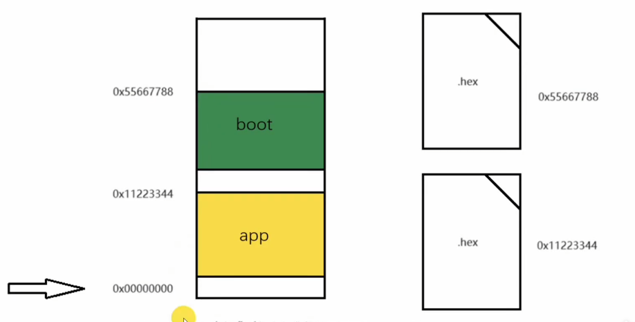
我们将第一个项目代码称之为 Bootloader 程序,第二个项目代码称之为 APP 程序,他们存 放在 STM32F407 FLASH 的不同地址范围,一般从最低地址区开始存放 Bootloader,紧跟其后 的就是 APP 程序(注意,如果 FLASH 容量足够,是可以设计很多 APP 程序的,本章我们只讨 论一个 APP 程序的情况)。
这样我们就是要实现 2 个程序:Bootloader 和 APP。 STM32F407 的 APP 程序不仅可以放到 FLASH 里面运行,也可以放到 SRAM 里面运行, 本章,我们将制作两个 APP,一个用于 FLASH 运行,一个用于内部 SRAM 运行。 我们先来看看 STM32F407 正常的程序运行流程(为了方便说明 IAP 过程,我们先仅考虑 代码全部存放在内部 FLASH 的情况),如图 62.1.1 所示

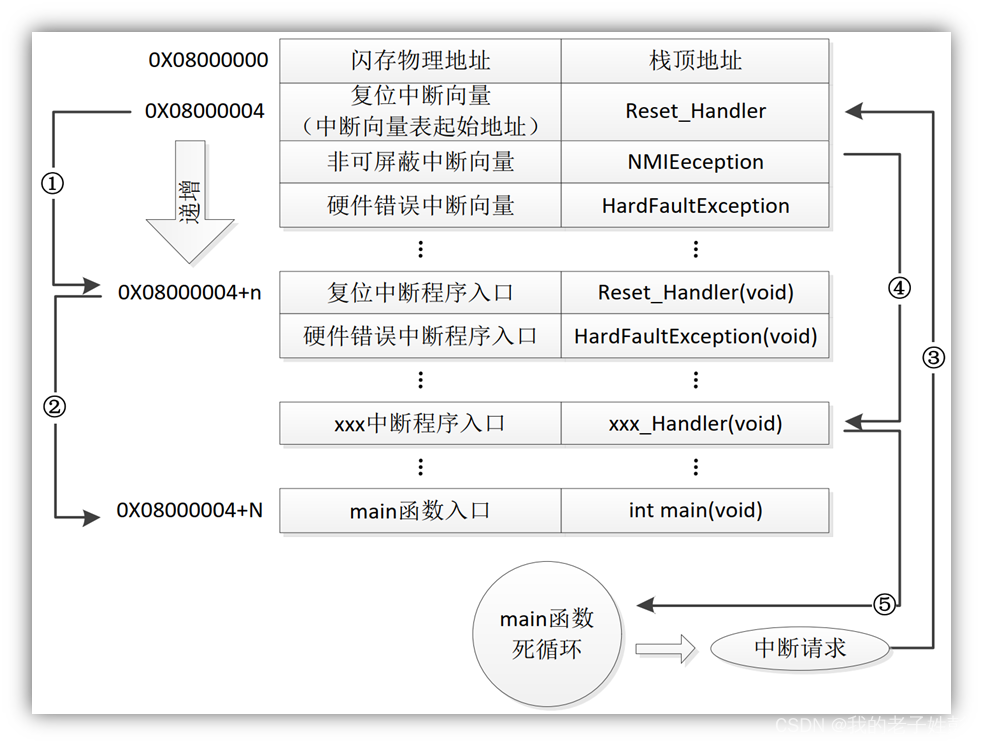
STM32F407 的内部闪存(FLASH)地址起始于 0x0800 0000,一般情况下,程序文件就从 此地址开始写入。此外 STM32F407 是基于 Cortex-M4 内核的微控制器,其内部通过一张“中断 向量表”来响应中断,程序启动后,将首先从“中断向量表”取出复位中断向量执行复位中断 程序完成启动,而这张“中断向量表”的起始地址是 0x0800 0004,当中断来临,STM32F407 的 内部硬件机制亦会自动将 PC 指针定位到“中断向量表”处,并根据中断源取出对应的中断向 量执行中断服务程序。
在图 62.1.1 中,STM32F407 在复位后,先从 0x08000004 地址取出复位中断向量的地址, 并跳转到复位中断服务程序,如图标号①所示;在复位中断服务程序执行完之后,会跳转到我 们的 main 函数,如图标号②所示;而我们的 main 函数一般都是一个死循环,在 main 函数执行 过程中,如果收到中断请求(发生了中断),此时 STM32F407 强制将 PC 指针指回中断向量表 处,如图标号③所示;然后,根据中断源进入相应的中断服务程序,如图标号④所示;在执行 完中断服务程序以后,程序再次返回 main 函数执行,如图标号⑤所示。 当加入 IAP 程序之后,程序运行流程如图 62.1.2 所示:

在图 62.1.2 所示流程中,STM32F407 复位后,还是从 0x08000004 地址取出复位中断向量 的地址,并跳转到复位中断服务程序,在运行完复位中断服务程序之后跳转到 IAP 的 main 函 数,如图标号①所示,此部分同图 62.1.1 一样;在执行完 IAP 以后(即将新的 APP 代码写入 STM32F407 的 FLASH,灰底部分。新程序的复位中断向量起始地址为 0x08000004+N+M),跳 转至新写入程序的复位向量表,取出新程序的复位中断向量的地址,并跳转执行新程序的复位 中断服务程序,随后跳转至新程序的 main 函数,如图标号②和③所示,同样 main 函数为一个 死循环,并且注意到此时 STM32F407 的 FLASH,在不同位置上,共有两个中断向量表。
在 main 函数执行过程中,如果 CPU 得到一个中断请求,PC 指针仍然会强制跳转到地址 0x08000004 中断向量表处,而不是新程序的中断向量表,如图标号④所示;程序再根据我们设 置的中断向量表偏移量,跳转到对应中断源新的中断服务程序中,如图标号⑤所示;在执行完 中断服务程序后,程序返回 main 函数继续运行,如图标号⑥所示。 通过以上两个过程的分析,我们知道 IAP 程序必须满足两个要求:
1) 新程序必须在 IAP 程序之后的某个偏移量为 x 的地址开始;
2) 必须将新程序的中断向量表相应的移动,移动的偏移量为 x;
本章,我们有 2 个 APP 程序:
1,FLASH APP 程序,即只运行在内部 FLASH 的 APP 程序。
2,SRAM APP 程序,即只运行在内部 SRAM 的 APP 程序,其运行过程和图 62.1.2 相似, 不过需要设置向量表的地址为 SRAM 的地址。
更改起始位置
FLASH
APP 程序使用以前例程即可,不需要对程序进行修改。 默认的条件下,图中 IROM1 的起始地址(Start)一般为 0x08000000,大小(Size)为 0x100000, 即从 0x08000000 开始的 1024K 空间为我们的程序存储区。

我们设置起始地址(Start)为 0x08004000,即偏移量为 0x4000(设置好 Start 和 Size,就完成 APP 程序的起始地址设置。IRAM 是 内存的地址,APP 可以独占这些内存,我们不需要修改。
注意:需要确保 APP 起始地址在 Bootloader 程序结束位置之后,并且偏移量为 0x200 的倍 数即可(相关知识,请参考:http://www.openedv.com/posts/list/392.htm)。
SRAM

这里我们将 IROM1 的起始地址(Start)定义为:0x20001000,大小为 0x19000(100K 字 节),即从地址 0x20000000 偏移 0x1000 开始,存放 SRAM APP 代码。这个分配关系大家可以 根据自己的实际情况修改,
由于 STM32F407ZGT6 只有一个 128K(不算 CCM)的片内 SRAM, 存放程序的位置与变量的加载位置不能重复,所以我们需要设置 IRAM1 中的地址(SRAM)的 起始地址变为 0x2001A000,分配大小只有 0x6000(24K 字节)。
整个 STM32F407ZGT6 的 SRAM (不含 CCM)分配情况为:最开始的 4K 给 Bootloader 程序使用,随后的 100K 存放 APP 程序, 最后 24K,用作 APP 程序的内存。 关于 APP 起始地址的设置方法,我们就介绍到这里,大家可以根据自己项目的实际需求进 行修改。
生成BIN文件
$K\ARM\ARMCC\bin\fromelf.exe --bin --output=Bin@L.bin !L这是一条生成bin文件的指令
使用方法如下

在小魔术棒中打到User页面
在下方的After Build/Rebuild 中将指令CV 进 Run#1 并打✔️,点击OK
在编译结束的时候出现
After Build - User command #1: D:\APP\Keil5\\ARM\ARMCC\bin\fromelf.exe --bin --output=BinTemplate.bin ..\..\Output\Template.axf
证明生成BIN文件成功 。

串口接收BIN文件
bin文件是二进制文件,和串口接收数据包差不多。
串口接收的代码如下
#define USART_REC_LEN               120*1024        /* 定义最大接收字节数 200 */
#define USART_EN_RX                 1               /* 使能(1)/禁止(0)串口1接收 */


#if USART_EN_RX     /* 如果使能了接收 */

#if !(__ARMCC_VERSION >= 6010050)   /* 不是AC6编译器,即使用AC5编译器时 */

/* 接收缓冲, 最大USART_REC_LEN个字节. */
uint8_t g_usart_rx_buf[USART_REC_LEN] __attribute__ ((at(0X20001000))); /* 指定数组位置 */

#else      /* 使用AC6编译器时 */

/* 接收缓冲, 最大USART_REC_LEN个字节. */
uint8_t g_usart_rx_buf[USART_REC_LEN] __attribute__((section(".bss.ARM.__at_0X20001000"))); /* 指定数组位置 */

#endif


uint32_t g_usart_rx_cnt = 0;


void USART_UX_IRQHandler(void)
{
    uint8_t rxdata;


   	if(USART_GetFlagStatus(USART1,USART_IT_RXNE)==SET)                /* 接收到数据 */
    {
        rxdata =  USART_ReceiveData(USART1);

        if (g_usart_rx_cnt < USART_REC_LEN)     /* 接收未满 */
        {
            g_usart_rx_buf[g_usart_rx_cnt] = rxdata;    /* 存储数据到 g_usart_rx_buf */
            g_usart_rx_cnt++;                           /* 计数加1 */
        }
    }


}
#endif
为了便于测试,我们定义一个大的接收数组 g_usart_rx_buf[USART_REC_LEN],
并保证这个数组能接收并缓存一个完整的 bin 文件,程序中 我们定了了这个大小为 120KB,因为我们有 SRAM 程序(47KB),所以把这部分的数组放用 __attribute__ ((at(0x20001000)))直接放到 SRAM 程序的位置,这样接收完成的 SRAM 程序后我 们直接跳转就可以了。
相当于直接把数组定义在内部SRAM地址中。
在主程序中需要判断串口接收是否完成。
主函数中的接收判断如下
  uint32_t oldcount = 0;                      /* 老的串口接收数据值 */
  uint32_t applenth = 0;                      /* 接收到的app代码长度 */


if (oldcount == g_usart_rx_cnt)   /* 新周期内,没有收到任何数据,认为本次数据接收完成 */
      {
        applenth = g_usart_rx_cnt;
        oldcount = 0;
        g_usart_rx_cnt = 0;
        printf("用户程序接收完成!\r\n");
        printf("代码长度:%dBytes\r\n", applenth);
				a=1;
      }
      else oldcount = g_usart_rx_cnt;
    }
		  delay_ms(500);
这里用 oldcount 的数字大小于g_usart_rx_cnt做对比,如果相等就代表接收完成。
注意每一轮判断结束之后需要 delay_ms(500); 延时一段时间,否则接受过程中会出现很多个 oldcount == g_usart_rx_cnt ,不能精准判断是否接收完成。
( 代码调试得来的经验。)
设置中断偏移
在APP函数中进行中断偏移,因为偏移量前面的被 Bootloader 占用了。
VTOR 寄存器存放的是中断向量表的起始地址。
默认的情况它由 BOOT 的启动模式决定, 对于 STM32F407 来说就是指向 0x0800 0000 这个位置,也就是从默认的启动位置加载中断向量 等信息,不过 ST 允许重定向这个位置,这样就可以从 Flash 区域的任意位置启动我们的代码了。
正点原子将其封装为函数void sys_nvic_set_vector_table(uint32_t baseaddr, uint32_t offset)
/**
 * @brief       设置中断向量表偏移地址
 * @param       baseaddr: 基址
 * @param       offset: 偏移量(必须是0, 或者0X100的倍数)
 * @retval      无
 */
void sys_nvic_set_vector_table(uint32_t baseaddr, uint32_t offset)
{
    /* 设置NVIC的向量表偏移寄存器,VTOR低9位保留,即[8:0]保留 */
    SCB->VTOR = baseaddr | (offset & (uint32_t)0xFFFFFE00);
}
设置 FLASH APP
sys_nvic_set_vector_table(FLASH_BASE, 0x10000);
设置 SRAM APP
#ifdef  VECT_TAB_RAM
    sys_nvic_set_vector_table(SRAM_BASE, 0x1000);
#else
    sys_nvic_set_vector_table(FLASH_BASE, 0x0);
#endif
这是正点原子设置中断偏移的方法,
简单粗暴
其实本质上就是修改VTOR 寄存器的数值,直接应用下面代码在MAIN函数第一行就行了,当然下面为FLASH时的中断偏移情况。
SCB->VTOR = FLASH_BASE | 0x4000;//设置中断偏移量int main(void)
{
SCB->VTOR = FLASH_BASE | 0x4000;//设置中断偏移量
Debug_USART_Config();
LED_GPIO_Config();
printf ("正在执行APP2\r\n");
/* 初始化基本定时器定时,0.5s产生一次中断 */
//TIMx_Configuration();
LED_RED;
//LED_GREEN;
// LED_BLUE;
//LED_PURPLE;
//LED_WHITE;
while(1)
{
}
}作用
将中断向量表向下进行偏移,偏移量为代码起始位置相对于0X80000000 移动的距离。

比如这个程序的起始位置为 0x8004000,则需要偏移 4000 .
不加这条代码也能正常跳转,但是会导致APP函数中的中断功能失效。
比如我在APP中代码写了一个定时器中断更改LED电平使其闪烁,如果不加就没有现象产生,加了就正常。
内部FLASH及相关标准库函数
解锁函数
void FLASH_Unlock(void)
{
  if((FLASH->CR & FLASH_CR_LOCK) != RESET)
  {
    /* Authorize the FLASH Registers access */
    FLASH->KEYR = FLASH_KEY1;
    FLASH->KEYR = FLASH_KEY2;
  }
}


#define FLASH_KEY1               ((uint32_t)0x45670123)
#define FLASH_KEY2               ((uint32_t)0xCDEF89AB)
由于内部 FLASH 空间主要存储的是应用程序,是非常关键的数据,为了防止误操作修改了这些 内容,芯片复位后默认会给 FLASH 上锁,这个时候不允许设置 FLASH 的控制寄存器,并且不能 对修改 FLASH 中的内容。
所以对 FLASH 写入数据前,需要先给它解锁。解锁的操作步骤如下:
(1) 往 Flash 密钥寄存器 FLASH_KEYR 中写入 KEY1 = 0x45670123
(2) 再往 Flash 密钥寄存器 FLASH_KEYR 中写入 KEY2 = 0xCDEF89AB
上锁
void FLASH_Lock(void)
{
  /* Set the LOCK Bit to lock the FLASH Registers access */
  FLASH->CR |= FLASH_CR_LOCK;
}
设置操作位数及擦除扇区
/**
  * @brief  Erases a specified FLASH Sector.
  *
  * @note   If an erase and a program operations are requested simultaneously,
  *         the erase operation is performed before the program one.
  *
  * @param  FLASH_Sector: The Sector number to be erased.
  *
  *  @note  For STM32F405xx/407xx and STM32F415xx/417xx devices this parameter can
  *         be a value between FLASH_Sector_0 and FLASH_Sector_11.
  *
  *         For STM32F42xxx/43xxx devices this parameter can be a value between
  *         FLASH_Sector_0 and FLASH_Sector_23.
  *
  *         For STM32F401xx devices this parameter can be a value between
  *         FLASH_Sector_0 and FLASH_Sector_5.
  *
  *         For STM32F411xE and STM32F412xG devices this parameter can be a value between
  *         FLASH_Sector_0 and FLASH_Sector_7.
  *
  *         For STM32F410xx devices this parameter can be a value between
  *         FLASH_Sector_0 and FLASH_Sector_4.
  *
  *         For STM32F413_423xx devices this parameter can be a value between
  *         FLASH_Sector_0 and FLASH_Sector_15.
  *
  * @param  VoltageRange: The device voltage range which defines the erase parallelism.
  *          This parameter can be one of the following values:
  *            @arg VoltageRange_1: when the device voltage range is 1.8V to 2.1V,
  *                                  the operation will be done by byte (8-bit)
  *            @arg VoltageRange_2: when the device voltage range is 2.1V to 2.7V,
  *                                  the operation will be done by half word (16-bit)
  *            @arg VoltageRange_3: when the device voltage range is 2.7V to 3.6V,
  *                                  the operation will be done by word (32-bit)
  *            @arg VoltageRange_4: when the device voltage range is 2.7V to 3.6V + External Vpp,
  *                                  the operation will be done by double word (64-bit)
  *
  * @retval FLASH Status: The returned value can be: FLASH_BUSY, FLASH_ERROR_PROGRAM,
  *                       FLASH_ERROR_WRP, FLASH_ERROR_OPERATION or FLASH_COMPLETE.
  */
FLASH_Status FLASH_EraseSector(uint32_t FLASH_Sector, uint8_t VoltageRange)
{
  uint32_t tmp_psize = 0x0;
  FLASH_Status status = FLASH_COMPLETE;

  /* Check the parameters */
  assert_param(IS_FLASH_SECTOR(FLASH_Sector));
  assert_param(IS_VOLTAGERANGE(VoltageRange));

  if(VoltageRange == VoltageRange_1)
  {
     tmp_psize = FLASH_PSIZE_BYTE;
  }
  else if(VoltageRange == VoltageRange_2)
  {
    tmp_psize = FLASH_PSIZE_HALF_WORD;
  }
  else if(VoltageRange == VoltageRange_3)
  {
    tmp_psize = FLASH_PSIZE_WORD;
  }
  else
  {
    tmp_psize = FLASH_PSIZE_DOUBLE_WORD;
  }
  /* Wait for last operation to be completed */
  status = FLASH_WaitForLastOperation();

  if(status == FLASH_COMPLETE)
  {
    /* if the previous operation is completed, proceed to erase the sector */
    FLASH->CR &= CR_PSIZE_MASK;
    FLASH->CR |= tmp_psize;
    FLASH->CR &= SECTOR_MASK;
    FLASH->CR |= FLASH_CR_SER | FLASH_Sector;
    FLASH->CR |= FLASH_CR_STRT;

    /* Wait for last operation to be completed */
    status = FLASH_WaitForLastOperation();

    /* if the erase operation is completed, disable the SER Bit */
    FLASH->CR &= (~FLASH_CR_SER);
    FLASH->CR &= SECTOR_MASK;
  }
  /* Return the Erase Status */
  return status;
}
本函数包含两个输入参数,分别是要擦除的扇区号和工作电压范围,选择不同电压时实质是选择 不同的数据操作位数,参数中可输入的宏在注释里已经给出。
函数根据输入参数配置 PSIZE 位, 然后擦除扇区,擦除扇区的时候需要等待一段时间,它使用 FLASH_WaitForLastOperation 等待, 擦除完成的时候才会退出 FLASH_EraseSector 函数。
第一个参数 FLASH_Sector 可以用野火的方法获取
/**
  * @brief  根据输入的地址给出它所在的sector
  *					例如:
						uwStartSector = GetSector(FLASH_USER_START_ADDR);
						uwEndSector = GetSector(FLASH_USER_END_ADDR);
  * @param  Address:地址
  * @retval 地址所在的sector
  */
static uint32_t GetSector(uint32_t Address)
{
  uint32_t sector = 0;

  if((Address < ADDR_FLASH_SECTOR_1) && (Address >= ADDR_FLASH_SECTOR_0))
  {
    sector = FLASH_Sector_0;
  }
  else if((Address < ADDR_FLASH_SECTOR_2) && (Address >= ADDR_FLASH_SECTOR_1))
  {
    sector = FLASH_Sector_1;
  }
  else if((Address < ADDR_FLASH_SECTOR_3) && (Address >= ADDR_FLASH_SECTOR_2))
  {
    sector = FLASH_Sector_2;
  }
  else if((Address < ADDR_FLASH_SECTOR_4) && (Address >= ADDR_FLASH_SECTOR_3))
  {
    sector = FLASH_Sector_3;
  }
  else if((Address < ADDR_FLASH_SECTOR_5) && (Address >= ADDR_FLASH_SECTOR_4))
  {
    sector = FLASH_Sector_4;
  }
  else if((Address < ADDR_FLASH_SECTOR_6) && (Address >= ADDR_FLASH_SECTOR_5))
  {
    sector = FLASH_Sector_5;
  }
  else if((Address < ADDR_FLASH_SECTOR_7) && (Address >= ADDR_FLASH_SECTOR_6))
  {
    sector = FLASH_Sector_6;
  }
  else if((Address < ADDR_FLASH_SECTOR_8) && (Address >= ADDR_FLASH_SECTOR_7))
  {
    sector = FLASH_Sector_7;
  }
  else if((Address < ADDR_FLASH_SECTOR_9) && (Address >= ADDR_FLASH_SECTOR_8))
  {
    sector = FLASH_Sector_8;
  }
  else if((Address < ADDR_FLASH_SECTOR_10) && (Address >= ADDR_FLASH_SECTOR_9))
  {
    sector = FLASH_Sector_9;
  }
  else if((Address < ADDR_FLASH_SECTOR_11) && (Address >= ADDR_FLASH_SECTOR_10))
  {
    sector = FLASH_Sector_10;
  }
  else /*((Address < FLASH_END_ADDR) && (Address >= ADDR_FLASH_SECTOR_11))*/
  {
    sector = FLASH_Sector_11;
  }


  return sector;
}
其中 ADDR_FLASH_SECTOR_0 ~ 12 均为基地址定义。这一点野火和正点原子的定义方法一样。
/* Base address of the Flash sectors */
#define ADDR_FLASH_SECTOR_0     ((uint32_t)0x08000000) /* Base address of Sector 0, 16 Kbytes   */
#define ADDR_FLASH_SECTOR_1     ((uint32_t)0x08004000) /* Base address of Sector 1, 16 Kbytes   */
#define ADDR_FLASH_SECTOR_2     ((uint32_t)0x08008000) /* Base address of Sector 2, 16 Kbytes   */
#define ADDR_FLASH_SECTOR_3     ((uint32_t)0x0800C000) /* Base address of Sector 3, 16 Kbytes   */
#define ADDR_FLASH_SECTOR_4     ((uint32_t)0x08010000) /* Base address of Sector 4, 64 Kbytes   */
#define ADDR_FLASH_SECTOR_5     ((uint32_t)0x08020000) /* Base address of Sector 5, 128 Kbytes  */
#define ADDR_FLASH_SECTOR_6     ((uint32_t)0x08040000) /* Base address of Sector 6, 128 Kbytes  */
#define ADDR_FLASH_SECTOR_7     ((uint32_t)0x08060000) /* Base address of Sector 7, 128 Kbytes  */
#define ADDR_FLASH_SECTOR_8     ((uint32_t)0x08080000) /* Base address of Sector 8, 128 Kbytes  */
#define ADDR_FLASH_SECTOR_9     ((uint32_t)0x080A0000) /* Base address of Sector 9, 128 Kbytes  */
#define ADDR_FLASH_SECTOR_10    ((uint32_t)0x080C0000) /* Base address of Sector 10, 128 Kbytes */
#define ADDR_FLASH_SECTOR_11    ((uint32_t)0x080E0000) /* Base address of Sector 11, 128 Kbytes */

#define ADDR_FLASH_SECTOR_12     ((uint32_t)0x08100000) /* Base address of Sector 12, 16 Kbytes  */
写入数据
(一个字节8个bit uint8_t大小为一个字节,最大值为2的八次方减一也就是255,uint16_t大小为两个字节)
对内部 FLASH 写入数据不像对外部 SRAM 操作那样直接指针操作就完成了,还要设置一系列的 寄存器,利用 FLASH_ProgramWord、FLASH_ProgramHalfWord 和 FLASH_ProgramByte 函数可按 字、半字及字节单位写入数据
/**
  * @brief  Programs a word (32-bit) at a specified address.
  *
  * @note   This function must be used when the device voltage range is from 2.7V to 3.6V.
  *
  * @note   If an erase and a program operations are requested simultaneously,
  *         the erase operation is performed before the program one.
  *
  * @param  Address: specifies the address to be programmed.
  *         This parameter can be any address in Program memory zone or in OTP zone.
  * @param  Data: specifies the data to be programmed.
  * @retval FLASH Status: The returned value can be: FLASH_BUSY, FLASH_ERROR_PROGRAM,
  *                       FLASH_ERROR_WRP, FLASH_ERROR_OPERATION or FLASH_COMPLETE.
  */
FLASH_Status FLASH_ProgramWord(uint32_t Address, uint32_t Data)
{
  FLASH_Status status = FLASH_COMPLETE;

  /* Check the parameters */
  assert_param(IS_FLASH_ADDRESS(Address));

  /* Wait for last operation to be completed */
  status = FLASH_WaitForLastOperation();

  if(status == FLASH_COMPLETE)
  {
    /* if the previous operation is completed, proceed to program the new data */
    FLASH->CR &= CR_PSIZE_MASK;
    FLASH->CR |= FLASH_PSIZE_WORD;
    FLASH->CR |= FLASH_CR_PG;

    *(__IO uint32_t*)Address = Data;

    /* Wait for last operation to be completed */
    status = FLASH_WaitForLastOperation();

    /* if the program operation is completed, disable the PG Bit */
    FLASH->CR &= (~FLASH_CR_PG);
  }
  /* Return the Program Status */
  return status;
}
看函数代码可了解到,使用指针进行赋值操作前设置了数据操作宽度,并设置了 PG 寄存器位, 在赋值操作后,调用了 FLASH_WaitForLastOperation 函数等待写操作完毕。HalfWord 和 Byte 操 作宽度的函数执行过程类似。
检测FLASH的状态
/**
  * @brief  Returns the FLASH Status.
  * @param  None
  * @retval FLASH Status: The returned value can be: FLASH_BUSY, FLASH_ERROR_PROGRAM,
  *                       FLASH_ERROR_WRP, FLASH_ERROR_RD, FLASH_ERROR_OPERATION or FLASH_COMPLETE.
  */
FLASH_Status FLASH_GetStatus(void)
{
  FLASH_Status flashstatus = FLASH_COMPLETE;

  if((FLASH->SR & FLASH_FLAG_BSY) == FLASH_FLAG_BSY)
  {
    flashstatus = FLASH_BUSY;
  }
  else
  {
    if((FLASH->SR & FLASH_FLAG_WRPERR) != (uint32_t)0x00)
    {
      flashstatus = FLASH_ERROR_WRP;
    }
    else
    {
      if((FLASH->SR & FLASH_FLAG_RDERR) != (uint32_t)0x00)
      {
        flashstatus = FLASH_ERROR_RD;
      }
      else
      {
        if((FLASH->SR & (uint32_t)0xE0) != (uint32_t)0x00)
        {
          flashstatus = FLASH_ERROR_PROGRAM;
        }
        else
        {
          if((FLASH->SR & FLASH_FLAG_OPERR) != (uint32_t)0x00)
          {
            flashstatus = FLASH_ERROR_OPERATION;
          }
          else
          {
            flashstatus = FLASH_COMPLETE;
          }
        }
      }
    }
  }
  /* Return the FLASH Status */
  return flashstatus;
}
FLASH->SR 寄存器状态宏定义
#define FLASH_FLAG_EOP                 ((uint32_t)0x00000001)  /*!< FLASH End of Operation flag               */
#define FLASH_FLAG_OPERR               ((uint32_t)0x00000002)  /*!< FLASH operation Error flag                */
#define FLASH_FLAG_WRPERR              ((uint32_t)0x00000010)  /*!< FLASH Write protected error flag          */
#define FLASH_FLAG_PGAERR              ((uint32_t)0x00000020)  /*!< FLASH Programming Alignment error flag    */
#define FLASH_FLAG_PGPERR              ((uint32_t)0x00000040)  /*!< FLASH Programming Parallelism error flag  */
#define FLASH_FLAG_PGSERR              ((uint32_t)0x00000080)  /*!< FLASH Programming Sequence error flag     */
#define FLASH_FLAG_RDERR               ((uint32_t)0x00000100)  /*!< Read Protection error flag (PCROP)        */
#define FLASH_FLAG_BSY                 ((uint32_t)0x00010000)  /*!< FLASH Busy flag                           */
等待FLASH操作完成
FLASH_Status FLASH_WaitForLastOperation(void)
{
  __IO FLASH_Status status = FLASH_COMPLETE;

  /* Check for the FLASH Status */
  status = FLASH_GetStatus();

  /* Wait for the FLASH operation to complete by polling on BUSY flag to be reset.
     Even if the FLASH operation fails, the BUSY flag will be reset and an error
     flag will be set */
  while(status == FLASH_BUSY)
  {
    status = FLASH_GetStatus();
  }
  /* Return the operation status */
  return status;
}
正点原子操作寄存器
解锁和上锁
**
 * @brief       解锁STM32的FLASH
 * @param       无
 * @retval      无
 */
static void stmflash_unlock(void)
{
    FLASH->KEYR = STM32_FLASH_KEY1;     /* FLASH 写入解锁序列. */
    FLASH->KEYR = STM32_FLASH_KEY2;
}


/* FLASH解锁键值 */
#define STM32_FLASH_KEY1               0X45670123
#define STM32_FLASH_KEY2               0XCDEF89AB


/**
 * @brief       flash上锁
 * @param       无
 * @retval      无
 */
static void stmflash_lock(void)
{
    FLASH->CR |= (uint32_t)1 << 31;     /* FLASH 上锁 */
}
获取 FLASH->SR 寄存器的数值来得到FLASH的错误状态
/**
 * @brief       得到FLASH的错误状态
 * @param       无
 * @retval      执行结果
 *   @arg       0   : 已完成
 *   @arg       其他 : 错误编号
 */
static uint8_t stmflash_get_error_status(void)
{
    uint32_t res = 0;
    res = FLASH->SR;

    if (res & (1 << 16)) return 1;  /* BSY=1, 繁忙 */
    if (res & (1 << 7))  return 2;  /* PGSERR=1,编程序列错误 */
    if (res & (1 << 6))  return 3;  /* PGPERR=1,编程并行位数错误 */
    if (res & (1 << 5))  return 4;  /* PGAERR=1,编程对齐错误 */
    if (res & (1 << 4))  return 5;  /* WRPERR=1,写保护错误 */

    return 0;   /* 没有任何状态/操作完成. */
}
等待操作完成
/**
 * @brief       等待操作完成
 * @param       time : 要延时的长短
 * @retval      执行结果
 *   @arg       0   : 已完成
 *   @arg       0XFF: 超时
 *   @arg       其他 : 错误编号
 */
static uint8_t stmflash_wait_done(uint32_t time)
{
    uint8_t res;

    do
    {
        res = stmflash_get_error_status();

        if (res != 1)
        {
            break;      /* 非忙, 无需等待了, 直接退出 */
        }

        time--;
    } while (time);

    if (time == 0)res = 0XFF;   /* 超时 */

    return res;
}
擦除扇区
/**
 * @brief       擦除扇区
 * @param       saddr   : 扇区地址 0 ~ 11
 *                        0~3, 16K扇区; 4,64K扇区; 5~11, 128K扇区.
 * @retval      执行结果
 *   @arg       0   : 已完成
 *   @arg       0XFF: 超时
 *   @arg       其他 : 错误编号
 */
static uint8_t stmflash_erase_sector(uint32_t saddr)
{
    uint8_t res = 0;

    res = stmflash_wait_done(0XFFFFFFFF);   /* 等待上次操作结束 */

    if (res == 0)
    {
        FLASH->CR &= ~(3 << 8);             /* 清除PSIZE原来的设置 */
        FLASH->CR |= 2 << 8;                /* 设置为32bit宽,确保VCC=2.7~3.6V之间!! */
        FLASH->CR &= ~(0X1F << 3);          /* 清除原来的设置 */
        FLASH->CR |= saddr << 3;            /* 设置要擦除的扇区 */
        FLASH->CR |= 1 << 1;                /* 扇区擦除 */
        FLASH->CR |= 1 << 16;               /* 开始擦除 */
        res = stmflash_wait_done(0XFFFFFFFF);   /* 等待操作结束 */

        if (res != 1)                       /* 非忙 */
        {
            FLASH->CR &= ~(1 << 1);         /* 清除扇区擦除标志 */
        }
    }

    return res;
}
输入参数为扇区号
和库函数一样,需要有一个寻址函数配套使用,该函数参数和库函数一样序号通过扇区查找函数来确定地址所在的扇区,不同的是正点原子的该擦除函数的输入参数通常为 0 ~ 11
而库函数的参数格式为 FLASH_Sector_0 ~ 11 。
同时库函数对于擦除字节的大小根据第二个参数 uint8_t VoltageRange 来确定,
@arg VoltageRange_1: when the device voltage range is 1.8V to 2.1V,
  *                                  the operation will be done by byte (8-bit)
  *@arg VoltageRange_2: when the device voltage range is 2.1V to 2.7V,
  *                                  the operation will be done by half word (16-bit)
  *@arg VoltageRange_3: when the device voltage range is 2.7V to 3.6V,
  *                                  the operation will be done by word (32-bit)
  *@arg VoltageRange_4: when the device voltage range is 2.7V to 3.6V + External Vpp,
  *                                  the operation will be done by double word (64-bit)
uint8_t stmflash_get_flash_sector(uint32_t addr)为正点原子为其配套的寻找扇区函数。
获取扇区号
/**
 * @brief       获取某个地址所在的flash扇区
 * @param       faddr   : flash地址
 * @retval      0~11, 即addr所在的扇区
 */
static uint8_t stmflash_get_flash_sector(uint32_t addr)
{
    if (addr < ADDR_FLASH_SECTOR_1)return 0;
    else if (addr < ADDR_FLASH_SECTOR_2)return 1;
    else if (addr < ADDR_FLASH_SECTOR_3)return 2;
    else if (addr < ADDR_FLASH_SECTOR_4)return 3;
    else if (addr < ADDR_FLASH_SECTOR_5)return 4;
    else if (addr < ADDR_FLASH_SECTOR_6)return 5;
    else if (addr < ADDR_FLASH_SECTOR_7)return 6;
    else if (addr < ADDR_FLASH_SECTOR_8)return 7;
    else if (addr < ADDR_FLASH_SECTOR_9)return 8;
    else if (addr < ADDR_FLASH_SECTOR_10)return 9;
    else if (addr < ADDR_FLASH_SECTOR_11)return 10;

    return 11;
}
读写内部 FLASH 不需要用到任何外部硬件,不过在擦写时常常需要知道各个扇区的基地址,我们把这些基地址自行定义。
/* FLASH 扇区的起始地址 */
#define ADDR_FLASH_SECTOR_0     ((uint32_t )0x08000000)     /* 扇区0起始地址, 16 Kbytes */
#define ADDR_FLASH_SECTOR_1     ((uint32_t )0x08004000)     /* 扇区1起始地址, 16 Kbytes */
#define ADDR_FLASH_SECTOR_2     ((uint32_t )0x08008000)     /* 扇区2起始地址, 16 Kbytes */
#define ADDR_FLASH_SECTOR_3     ((uint32_t )0x0800C000)     /* 扇区3起始地址, 16 Kbytes */
#define ADDR_FLASH_SECTOR_4     ((uint32_t )0x08010000)     /* 扇区4起始地址, 64 Kbytes */
#define ADDR_FLASH_SECTOR_5     ((uint32_t )0x08020000)     /* 扇区5起始地址, 128 Kbytes */
#define ADDR_FLASH_SECTOR_6     ((uint32_t )0x08040000)     /* 扇区6起始地址, 128 Kbytes */
#define ADDR_FLASH_SECTOR_7     ((uint32_t )0x08060000)     /* 扇区7起始地址, 128 Kbytes */
#define ADDR_FLASH_SECTOR_8     ((uint32_t )0x08080000)     /* 扇区8起始地址, 128 Kbytes */
#define ADDR_FLASH_SECTOR_9     ((uint32_t )0x080A0000)     /* 扇区9起始地址, 128 Kbytes */
#define ADDR_FLASH_SECTOR_10    ((uint32_t )0x080C0000)     /* 扇区10起始地址,128 Kbytes */
#define ADDR_FLASH_SECTOR_11    ((uint32_t )0x080E0000)     /* 扇区11起始地址,128 Kbytes */
写入数据
在FLASH指定地址写一个字 (32位数据)
/**
 * @brief       在FLASH指定地址写一个字 (32位数据)
 *   @note      这了写入一个字, 是指4个字节
 * @param       faddr   : 写入地址 (此地址必须为4的倍数!!)
 * @param       data    : 要写入的数据(32位)
 * @retval      执行结果
 *   @arg       0   : 已完成
 *   @arg       0XFF: 超时
 *   @arg       其他 : 错误编号
 */
static uint8_t stmflash_write_word(uint32_t faddr, uint32_t data)
{
    uint8_t res;

    res = stmflash_wait_done(0XFFFFF);

    if (res == 0)   /* OK */
    {
        FLASH->CR &= ~(3 << 8);             /* 清除PSIZE原来的设置 */
        FLASH->CR |= 2 << 8;                /* 设置为32bit宽,确保VCC=2.7~3.6V之间!! */
        FLASH->CR |= 1 << 0;                /* 编程使能 */
        *(volatile uint32_t *)faddr = data; /* 写入数据 */
        res = stmflash_wait_done(0XFFFFF);  /* 等待操作完成,一个字编程 */

        if (res != 1)                       /* 操作成功 */
        {
            FLASH->CR &= ~(1 << 0);         /* 清除PG位 */
        }
    }

    return res;
}
在FLASH 指定位置, 写入指定长度的数据(自动擦除)
/**
 * @brief       在FLASH 指定位置, 写入指定长度的数据(自动擦除)
 *   @note      因为STM32F4的扇区实在太大,没办法本地保存扇区数据,所以本函数写地址如果非0XFF
 *              ,那么会先擦除整个扇区且不保存扇区数据.所以写非0XFF的地址,将导致整个扇区数据丢失.
 *              建议写之前确保扇区里没有重要数据,最好是整个扇区先擦除了,然后慢慢往后写.
 *              该函数对OTP区域也有效!可以用来写OTP区!
 *              OTP区域地址范围:0X1FFF7800~0X1FFF7A0F(注意:最后16字节,用于OTP数据块锁定,别乱写!!)
 * @param       waddr   : 起始地址 (此地址必须为4的倍数!!,否则写入出错!)
 * @param       pbuf    : 数据指针
 * @param       length  : 要写入的 字(32位)数(就是要写入的32位数据的个数)
 * @retval      无
 */
void stmflash_write(uint32_t waddr, uint32_t *pbuf, uint32_t length)
{

    uint8_t status = 0;
    uint32_t addrx = 0;
    uint32_t endaddr = 0;

    if (waddr < STM32_FLASH_BASE || waddr % 4 ||        /* 写入地址小于 STM32_FLASH_BASE, 或不是4的整数倍, 非法. */
        waddr > (STM32_FLASH_BASE + STM32_FLASH_SIZE))  /* 写入地址大于 STM32_FLASH_BASE + STM32_FLASH_SIZE, 非法. */
    {
        return;
    }

    stmflash_unlock();              /* FLASH解锁 */

    FLASH->ACR &= ~(1 << 10);       /* FLASH擦除期间,必须禁止数据缓存!!!搞了我两晚上才发现这个问题!  将 某 数a 的 某 位 清 0 */
    addrx = waddr;                  /* 写入的起始地址 */
    endaddr = waddr + length * 4;   /* 写入的结束地址 */

    if (addrx < 0X1FFF0000)         /* 只有主存储区,才需要执行擦除操作!! */
    {
        while (addrx < endaddr)     /* 扫清一切障碍.(对非FFFFFFFF的地方,先擦除) */
        {
            if (stmflash_read_word(addrx) != 0XFFFFFFFF)    /* 有非0XFFFFFFFF的地方,要擦除这个扇区 */
            {
                status = stmflash_erase_sector(stmflash_get_flash_sector(addrx));

                if (status)break;   /* 发生错误了 */
            }
            else
            {
                addrx += 4;
            }
        }
    }

    if (status == 0)
    {
        while (waddr < endaddr)     /* 写数据 */
        {
            if (stmflash_write_word(waddr, *pbuf))  /* 写入数据 */
            {
                break;              /* 写入异常 */
            }

            waddr += 4;
            pbuf++;
        }
    }

    FLASH->ACR |= 1 << 10;          /* FLASH擦除结束,开启数据fetch */

    stmflash_lock();                /* 上锁 */
}
流程为解锁,循环擦除和循环写入,再上锁。
我尝试在这个函数中将正点原子的所有函数替换为库函数,其中解锁和上锁以及写入单个32位字节的函数都可以正常替换,但是stmflash_erase_sector(stmflash_get_flash_sector(addrx))替换为FLASH_Status FLASH_EraseSector(uint32_t FLASH_Sector, uint8_t VoltageRange)就一直不好使。也不知道因为啥,算了,就用正点原子的这个擦除代码吧。
读取数据
从指定地址读取一个字
/**
 * @brief       从指定地址读取一个字 (32位数据)
 * @param       faddr   : 读取地址 (此地址必须为4的倍数!!)
 * @retval      读取到的数据 (32位)
 */
uint32_t stmflash_read_word(uint32_t faddr)
{
    return *(volatile uint32_t *)faddr;
}
在指定地址中去读取指定长度数据
/**
 * @brief       从指定地址开始读出指定长度的数据
 * @param       raddr : 起始地址
 * @param       pbuf  : 数据指针
 * @param       length: 要读取的 字(32位)数(就是要读取的32位数据的个数)
 * @retval      无
 */
void stmflash_read(uint32_t raddr, uint32_t *pbuf, uint32_t length)
{
    uint32_t i;

    for (i = 0; i < length; i++)
    {
        pbuf[i] = stmflash_read_word(raddr);    /* 读取4个字节(1个字) */
        raddr += 4;                             /* 偏移4个字节 */
    }
}
以上为正点原子根据配置寄存器实现相关功能的所有代码。
IAP程序
以上对于FLASH操作的函数都是为了程序写入和程序跳转等相关函数服务的,接下来回到程序部分。
IAP写入APP BIN
uint32_t g_iapbuf[512];       /* 2K字节缓存 */


/**
 * @brief       IAP写入APP BIN
 * @param       appxaddr : 应用程序的起始地址
 * @param       appbuf   : 应用程序CODE
 * @param       appsize  : 应用程序大小(字节)
 * @retval      无
 */
void iap_write_appbin(uint32_t appxaddr, uint8_t *appbuf, uint32_t appsize)
{
    uint32_t t;
    uint16_t i = 0;
    uint32_t temp;
    uint32_t fwaddr = appxaddr; /* 当前写入的地址 */
    uint8_t *dfu = appbuf;

    for (t = 0; t < appsize; t += 4)
    {
        temp = (uint32_t)dfu[3] << 24;
        temp |= (uint32_t)dfu[2] << 16;
        temp |= (uint32_t)dfu[1] << 8;
        temp |= (uint32_t)dfu[0];
        dfu += 4;               /* 偏移2个字节 */
        g_iapbuf[i++] = temp;

        if (i == 512)
        {
            i = 0;
            stmflash_write(fwaddr, g_iapbuf, 512);
            fwaddr += 2048;     /* 偏移2048  16 = 2 * 8  所以要乘以2 */
        }
    }

    if (i)
    {
        stmflash_write(fwaddr, g_iapbuf, i);  /* 将最后的一些内容字节写进去 */
    }
}
参数分别为写入的地址,写入的数据 和 数据长度。在接收完bin文件之后,bin文件数据存储在串口接收的数组里。
这段代码中将*appbuf中的数据每32位为一组存储进缓存数组。之后用 stmflash_write(); 函数进行数据的写入,直至写完。
在保存了一个完整的 APP 到了对应的位置后,我们需要对栈顶进行检查操作,初步检查程 序设置正确再进行跳转。
我们以 Flash APP 为例,用 bin 文件查看工具(A 盘→6,软件资料→1, 软件→winhex),可以看到 bin 的内容默认为小端结构,如图 62.3.2.1 所示。

我们利用 STM32 的 bin 文件的特性,按 32 位取的数据,开始的第一个字为 SP 的地址,第 二个为 Reset_Handler 的地址,我们利用这个特性在跳转前做一个初步的判定,然后设置主堆 栈,这部分我们用到 sys.c 下的嵌入汇编函数 sys_msr_msp()
就是对 __set_MSP(addr); 函数进行一个封装。乞丐版直接定义直接用的。
/**
 * @brief       设置栈顶地址
 * @note        左侧的红X, 属于MDK误报, 实际是没问题的
 * @param       addr: 栈顶地址
 * @retval      无
 */
void sys_msr_msp(uint32_t addr)
{
    __set_MSP(addr);    /* 设置栈顶地址 */
}
跳转功能
跳转到应用程序段
正点原子
iapfun jump2app;
/**
* @brief 跳转到应用程序段(执行APP)
* @param appxaddr : 应用程序的起始地址
* @retval 无
*/
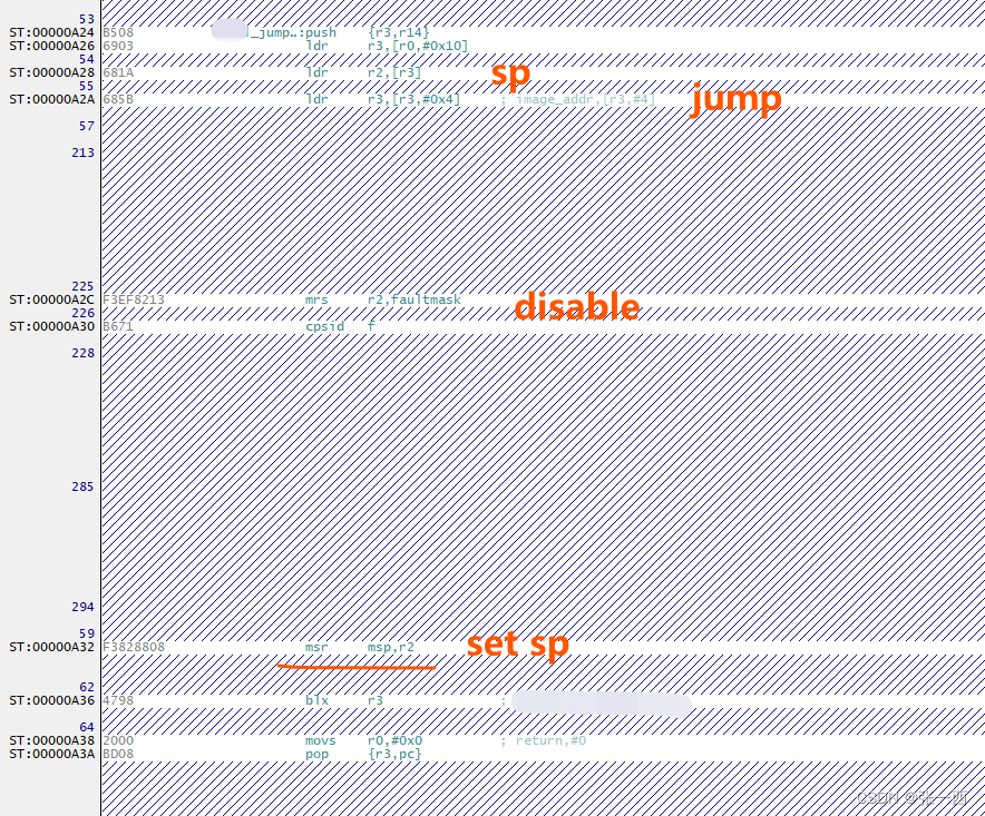
void iap_load_app(uint32_t appxaddr)
{
if (((*(volatile uint32_t *)appxaddr) & 0x2FFE0000) == 0x20000000) /* 检查栈顶地址是否合法.可以放在内部SRAM共64KB(0x20000000) */
{
/* 用户代码区第二个字为程序开始地址(复位地址) */
jump2app = (iapfun) * (volatile uint32_t *)(appxaddr + 4);
/* 初始化APP堆栈指针(用户代码区的第一个字用于存放栈顶地址) */
sys_msr_msp(*(volatile uint32_t *)appxaddr);
/* 跳转到APP */
jump2app();
}
}
博主加强版
iapfun jump2app;


//跳转到应用程序段
//appxaddr:用户代码起始地址
void iap_load_app(u32 appxaddr)
{
  unsigned char i = 0;
  if(((*(vu32*)appxaddr)&0x2FFE0000)==0x20000000)	//检查栈顶地址是否合法
  {
    /* 首地址是MSP,地址+4是复位中断服务程序地址 */
    jump2app=(iapfun)*(vu32*)(appxaddr+4);

    /* 关闭全局中断 */
    __set_PRIMASK(1);

    /* 关闭滴答定时器,复位到默认值 */
    SysTick->CTRL = 0;
    SysTick->LOAD = 0;
    SysTick->VAL = 0;

    /* 设置所有时钟到默认状态 */
    RCC_DeInit();

    /* 关闭所有中断,清除所有中断挂起标志 */
    for (i = 0; i < 8; i++)
    {
      NVIC->ICER[i]=0xFFFFFFFF;
      NVIC->ICPR[i]=0xFFFFFFFF;
    }

    /* 使能全局中断 */
    __set_PRIMASK(0);

    /* 在RTOS工程,这条语句很重要,设置为特权级模式,使用MSP指针 */
    __set_CONTROL(0);

    MSR_MSP(*(vu32*)appxaddr);					//初始化APP堆栈指针(用户代码区的第一个字用于存放栈顶地址)
    jump2app();									//跳转到APP.

    /* 跳转成功的话,不会执行到这里,用户可以在这里添加代码 */
    while (1)
    {

    }
  }
}
乞丐版
typedef  void (*pFunction)(void);     /*创建了一个类型别名 pFunction,它是一个指向无返回值且不
                                       带参数的函数指针类型*/
pFunction Jump_To_Application;        /*定义了一个名为 Jump_To_Application 的变量,它是一个函
                                      数指针,可以指向满足 pFunction 类型签名的函数。*/
uint32_t JumpAddress;                //用来装需要跳转的地址


void Jump2App(uint32_t appxaddr)     //跳转函数,用于跳转到用户应用程序,uint32_t appxaddr传参
                                        为需要跳转的程序地址。
{

//这一行首先检查用户代码是否已经被烧录到指定的地址(Application1Address)。
  if (((*(__IO uint32_t*)appxaddr) & 0x2FFE0000 ) == 0x20000000)
  {
    JumpAddress = *(__IO uint32_t*) (appxaddr + 4);
    Jump_To_Application = (pFunction) JumpAddress;
    __set_MSP(*(__IO uint32_t*) appxaddr);
    Jump_To_Application();   //跳转到用户应用程序的入口点

  }

}


//设置栈顶地址
//addr:栈顶地址
__asm void MSR_MSP(u32 addr)
{
  MSR MSP, r0 			//set Main Stack value
  BX r14
}
主函数
/**
  ******************************************************************************
  * @file    main.c
  * @author  fire
  * @version V1.0
  * @date    2015-xx-xx
  * @brief   基本定时器定时
  ******************************************************************************
  * @attention
  *
  * 实验平台:野火  STM32 F407 开发板
  * 论坛    :http://www.firebbs.cn
  * 淘宝    :https://fire-stm32.taobao.com
  *
  ******************************************************************************
  */

#include "stm32f4xx.h"
#include "./tim/bsp_basic_tim.h"
#include "bsp_debug_usart.h"
#include "./led/bsp_led.h"
#include "FLASH.h"
#include "delay.h"
#include "time.h"
#include "./key/bsp_key.h"

#define WaitTimeMs 3000 //等待时间,ms,boot程序启动后未在该时间内发起通讯自动跳转进入app程序
extern int TickMs;

uint8_t a=0;

/**
  * @brief  主函数
  * @param  无
  * @retval 无
  */
int main(void)
{
  int a = 0;

  uint32_t oldcount = 0;                      /* 老的串口接收数据值 */
  uint32_t applenth = 0;                      /* 接收到的app代码长度 */
  usart_init(84, 115200);
  delay_init();
  LED_GPIO_Config();
	TIMx_Configuration();
  Key_GPIO_Config();
  printf ("HELLO WORLD\r\n");
  LED_CYAN;
	//iap_load_app(FLASH_APP1_ADDR);

  while(1)
  {

		if( TickMs < WaitTimeMs ){ LED_CYAN;

    if (g_usart_rx_cnt)
    {
      if (oldcount == g_usart_rx_cnt)   /* 新周期内,没有收到任何数据,认为本次数据接收完成 */
      {
        applenth = g_usart_rx_cnt;
        oldcount = 0;
        g_usart_rx_cnt = 0;
        printf("用户程序接收完成!\r\n");
        printf("代码长度:%dBytes\r\n", applenth);
				a=1;
      }
      else oldcount = g_usart_rx_cnt;
    }
		  delay_ms(500);

		 }

		else { iap_load_app(FLASH_APP1_ADDR);  }


    if(	a==1)
    {
      if (applenth)
      {
        printf("开始更新固件...\r\n");


        if (((*(volatile uint32_t *)(0X20001000 + 4)) & 0xFF000000) == 0x08000000)  /* 判断是否为0X08XXXXXX */
        {
          iap_write_appbin(FLASH_APP1_ADDR ,g_usart_rx_buf, applenth);            /* 更新FLASH代码 */

          printf("固件更新完成!\r\n");
        }
        else
        {

          printf("非FLASH应用程序!\r\n");
        }
      }
      else
      {
        printf("没有可以更新的固件!\r\n");

      }

     delay_ms(500);


		 printf("flash addr :%x \r\n",(*(volatile uint32_t *)(FLASH_APP1_ADDR + 4)) & 0xFF000000);

      if (((*(volatile uint32_t *)(FLASH_APP1_ADDR + 4)) & 0xFF000000) == 0x08000000) /* 判断FLASH里面是否有APP,有的话执行 */
      {
        printf("开始执行FLASH用户代码!!\r\n\r\n");
        delay_ms(10);
        iap_load_app(FLASH_APP1_ADDR);/* 执行FLASH APP代码 */
      }
      else
      {
        printf("没有可以运行的固件!\r\n");

      }


    }

  }
}
这里对于我自己写的boot loader 进行一个讲解,首先我初始化了一个定时器作为时间判断,如果超过这个时间还没有收到上位机发来的程序,则判定为不需要升级,直接跳转到代码所在位置。
如果在设定时间之内接收到了数据,则在接收完成之后,更改变量 a 的数值。
从而自动进行固件更新和跳转。
实现效果为.........

分开总结及步骤合并
bootloader程序
1. 设置 bootloader 程序大小

2. 通过某种协议,串口,OTA,CAN 接收新代码的数据包
3.能跳转到APP位置执行APP功能
流程
1)检查是否需要对第二部分代码进行更新
2)如果不需要更新则转到 4)
3)执行更新操作
4)跳转到第二部分代码执行
app程序
1.设置中断偏移量,避免中断功能代码失效
2.完成 自定义的 APP功能任务
代码链接分享
这里分享两个代码
我自己根据正点原子的例程在野火代码的基础上改的(已实现)
链接:https://pan.baidu.com/s/1nD22FUhoE390d9oqHJiwfw?pwd=xwlj
提取码:xwlj
--来自百度网盘超级会员V3的分享
正点原子的例程(修改相关引脚和时钟参数在野火的板子上实现功能)
链接:https://pan.baidu.com/s/13xaiVEuSUIjN5dvfpetVBA?pwd=pjz9
提取码:pjz9
--来自百度网盘超级会员V3的分享
OK , 撤!!!


![【[STM32]标准库-自定义<span style='color:red;'>BootLoader</span>】](https://img-blog.csdnimg.cn/direct/a26461f3cf7e495a98c63cc9f1d595b2.png)